

It is important to optimize power supply design to improve efficiency. Improving efficiency not only saves energy and reduces heat generation, but also reduces the size of the power supply. (source: Easybom)
This article will discuss how to balance the number ratio of top-tube MOSFETs (HS-FETs) to bottom-tube MOSFETs (LS-FETs) to improve the efficiency of a power supply design.
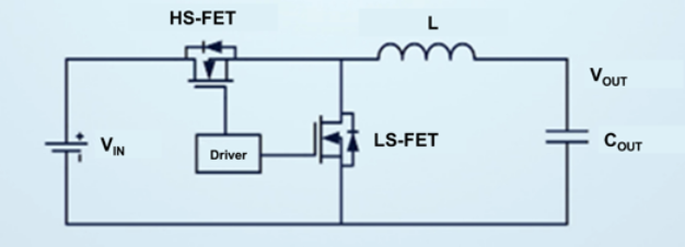
Figure 1 shows a simplified circuit with HS-FETs and LS-FETs.
When selecting MOSFETs, it is a challenge for power supply engineers to appropriately allocate the internal resistance of HS-FETs and LS-FETs for optimal efficiency.
MOSFET Structure and Loss Composition
The choice of a MOSFET is a matter of efficiency, and designers need to weigh its conduction losses against its switching losses. Conduction losses occur during MOSFET shutdown due to current flowing through the on-resistance; switching losses occur during MOSFET switching because the MOSFET does not switch instantaneously. These are caused by the capacitive behavior of the semiconductor structure within the MOSFET.
A MOSFET is an integrated multi-component structure consisting of multiple MOSFET semiconductor structures connected in parallel. The more MOSFET crystals connected in parallel, the lower the on-resistance (RDS(ON)), but the higher the parasitic capacitance. A smaller RDS(ON) reduces conduction losses, but increases parasitic capacitance, which increases switching losses. Therefore, designers need to strike a balance between resistance and capacitance. Selecting a MOSFET requires careful consideration, but deciding through on-board testing can take too much time and resources. Therefore, an accurate mathematical model to analyze losses and aid in MOSFET selection would be more valuable.
Calculating Conduction Loss
Let’s start with a relatively simple conduction loss calculation. The conduction loss can be calculated from the current and ripple current flowing through the MOSFET in a single cycle.
To ensure accuracy, this calculation takes into account the relationship between RDS(ON) and temperature. Because the internal resistance of a MOSFET, RDS(ON), is not a fixed value, it increases with temperature.
The calculation of conduction loss is shown in Figure 2. Where IO is the nominal current, ΔIO is the current ripple amplitude, TJ is the junction temperature, and k is the temperature coefficient.
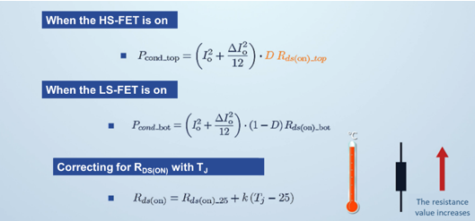
Figure 2: Calculation of conduction losses
Switching Losses (Parasitic Effects)
The calculation of switching loss is difficult because the parasitic inductance due to the inductance in each loop and the nonlinear parasitic capacitance of the MOSFET at different voltages need to be considered in the calculation.
Figure 3 shows the two parasitic factors that need to be considered in the switching loss calculation.
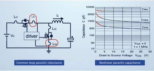
Figure 3: Two Parasitic Factors
Switching Losses (Conduction Losses)
The conduction loss consists of three stages, as described below:
Stage 1 (HS-FET stage): When the HS-FET conducts, the drain-source voltage (VDS) begins to drop and the drain-source current rises until the VDS(TOP) voltage of the HS-FET drops to 0V or the HS-FET current (IHS) rises to the output current (IOUT).
Stage 2 (Reverse Recovery Stage): During reverse recovery, ITOP peaks and then the LS-FET begins to generate voltage.
Stage 3 (Oscillation Stage): Oscillation ends when the IHS stops fluctuating.
Figure 4 shows the switching losses associated with the conduction losses.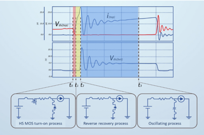
Figure 4: Conduction Losses
Switching losses (turn-off losses)
The turn-off loss consists of two phases as described below:
Stage 1 (DS Voltage Rise): The IDS falls as the VDS rises. This phase ends when the IDS drops to 0A.
Phase 2 (Oscillation): This phase ends when VDS stops oscillating.
Figure 5 shows the shutdown loss.
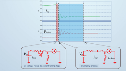
Figure 5: Shutdown Loss
Mathematical Model and Analytical Verification
Once the various losses of the circuit are understood, the mathematical model can be developed as follows:
Set the circuit parameter values as per requirement. Analyze the values of the MOSFETs based on the equations above and their nonlinear parameter compensation values.
Perform transient simulation by running at least one switching cycle during steady state operation of the converter.
Integrate the voltage and current waveforms to obtain the switching and conduction losses of the MOSFET. This step can be accomplished with a power probe or by multiplying the current and VDS waveforms.
Once modeled, use the data obtained from the power losses obtained above to obtain a simulated efficiency value, which is compared to the efficiency curve obtained from the board (or datasheet). The model is considered accurate if the error in the calculated efficiency is within 0.5% (see Figure 6).
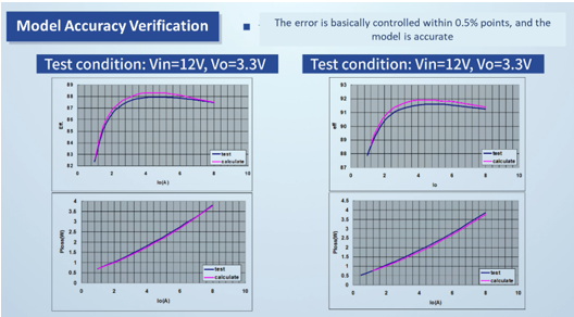
Figure 6: Mathematical Model Validation
MOSFET Selection Based on Mathematical Tools
In the examples in this paper, we use 10 MOSFETs with a total internal resistance of 100mΩ to calculate the efficiency curves at different up/down tube MOSFET ratios based on the model described above. For example, a ratio of 1:9 means that there is 1 HS-FET (high RDS(ON), low capacitance) and 9 LS-FETs (low RDS(ON), low capacitance).
By comparing the curves, we can conclude that the optimal ratio of MOSFETs for 12V to 3.3V, 10A applications is 3:7 (see Figure 7). This set of efficiency curves shows that even if the number of MOSFETs is the same, different ratios will result in different efficiency curves. From this we can find the optimal MOSFET ratio for the optimal efficiency curve.
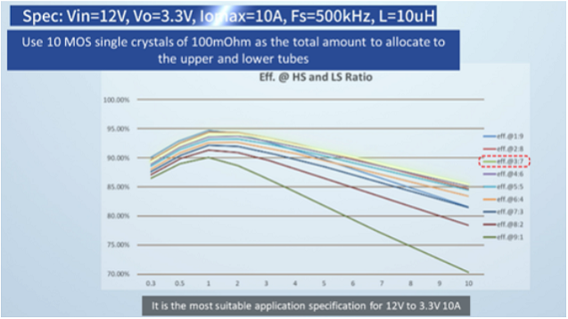
Figure 7: Optimal MOSFET Ratio
Figure 9 shows how to find the minimum loss point in a circuit with different MOSFET ratios for the same input and output specifications and the same output current. The designer must keep these specifications in mind when selecting the MOSFET ratio.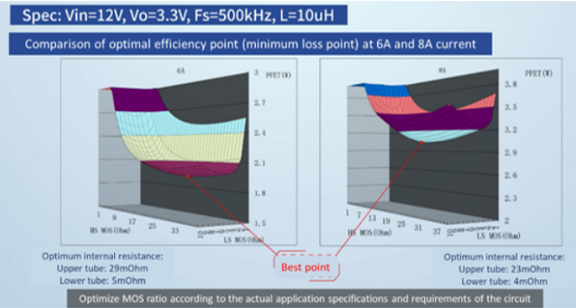
Figure 8: Comparison of optimal efficiency
To summarize
MOSFET selection is closely related to circuit efficiency, and accurate mathematical models can simplify the selection and design of MOSFET transistors. To obtain an accurate model, the parasitic parameters of the circuit need to be considered and efficiency curves need to be utilized to verify the results.