Know About the Application of Sapphire Substrate in the LED Sector
The discovery of allotropes like graphene has resulted in a significant increase in research and development efforts throughout the world, focusing on the discovery of novel two-dimensional (2D) materials. The search for novel materials was mostly reliant on laboratory operations, which were hampered by several obstacles, including producing a scalable volume of high-quality crystalline 2D materials. During the forecast period, get Sapphire substrate as this market is seeing the rising usage of the sapphire substrate in crystal.
Due to the increasing uses of sapphire substrates, research and development efforts are likely to increase in the future years. Furthermore, technical improvements and advancements in contemporary engineering are expected to continue to drive market expansion in the future years.
Get Sapphire Substrate which is being used in the LED sector. Sapphire has shown to be a versatile material that may be used in various applications, including LEDs, optical components, and RFICs. Sapphire has several physical properties that make it appropriate for various applications, including hardness and resistance to physical and chemical degradation. The markets that use sapphires, such as rising markets and expanding applications, significant market trends, and the migration to big diameter sapphire wafers, will be examined in this white paper.
The main end market for sapphire is LEDs. General illumination and LCD backlighting are the two most common end applications in that industry. Signage and automobiles are two more notable LED market sectors. Most LED manufacturers utilize a single production method for multiple or all applications, and they don’t take into account substrate demand by application. The benefits of sapphire, on the other hand, differ according to the application. For example, LEDs for mobile phones and laptops benefit from extended life, which is less important for LEDs for mobile handsets and notebooks, which favor great brightness and low power consumption.
Demand for Sapphire by Application
Although most people assume there is minimal correlation between LED application and sapphire substrate type; this is not the case. Customers might request more lasting LEDs based on the physical benefits of sapphire in terms of thermal matching and stable LED devices, for example, in applications where extended lifetime and dependability are essential, such as automotive, industrial, and lighting. Silicon may be more successful in consumer applications that require smaller, dimmer die with shorter lifetimes. Temperature resistance, history, dependability, yield, and quality, according to one respondent, are particularly important benefits for sapphire-based LEDs when utilized in general illumination.
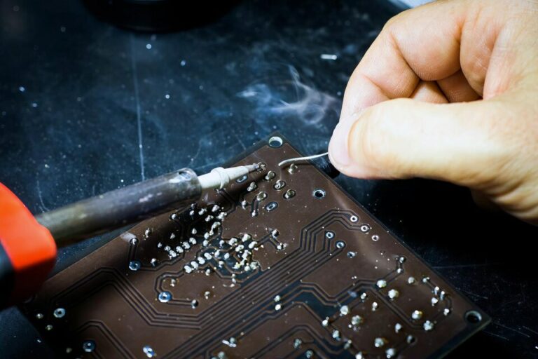
The chemicals that will constitute the emitting layer of the LED are deposited as vapor onto sapphire as part of the LED manufacturing process. The majority of today’s LEDs are made on a sapphire substrate.
-
Sapphire substrate in C-plane for LEDs
It is a sapphire substrate for LEDs that are widely used by many manufacturers for GaN growth, owing to the mature process, low cost, and stable physical and chemical properties of sapphire wafers grown along the C axis, and the technology is mature and stable when epitoxy is carried out on the C plane.
The most common substrate is C-plane sapphire. Professor Akasaki of Japan and Dr. Nakamura Shuji of Nichia broke through the challenges of lattice mismatch (buffer layer) between InGaN and sapphire substrate, p-type material activation, and other issues in 1993, and Nichia became the first company to create blue LED.
-
A sapphire substrate in the R-plane or M-plane for LEDs
To enhance luminous efficiency, it is mostly utilized to produce non-polar/semi-polar planar GaN epitaxial films. The c-axis is the polar axis of GaN. Thus the GaN epitaxial film produced on the sapphire substrate generally develops along the c-axis, which results in a high built-in electric field in the active layer quantum well GaN-based device, lowering the luminous efficiency. As a result, non-polar GaN epitaxy may be developed to circumvent this physical phenomenon and enhance luminescence efficiency.
-
Sapphire Substrate Pattern (PSS)
Nanoscale-specific regular micro-structure patterns are designed and made on a sapphire substrate using growth or etching to control the light output form of LED. The differential defects between GaN growing on the sapphire substrate can be reduced simultaneously, improving epitaxy quality, increasing the internal quantum efficiency of LED, and increasing the efficiency of light emitted.
Get Sapphire Substrate online which has evolved as a versatile material with a wide range of uses in a variety of sectors. Sapphire’s inherent physical properties of durability, light transmission, chemical inertness, and thermal insulation make it appealing to a wide range of markets, from LED optical windows, lenses, and covers to semiconductor applications in smartphones and other consumer electronics.
These advantages are important right now. Given the higher die size used, sapphire demand will increase as the lighting industry expands into a more major segment and larger, thicker wafers are used, leading to a predicted four years of 30%+ annual growth (by 2inch TIE in sapphire demand). The prediction takes into account the different thicknesses of bigger wafers.